
TSMC Aims to Restart 6T SRAM Scaling on the A14 Node at 0.017 Square Micrometers | ItInsightsWorld
Ask any design team how long cache footprints have been frozen and the answer points at TSMC's own record: after years of a stationary 6T cell, the vendor is finally signalling movement. On the current roadmap, the break comes with the A14 node, whose SRAM cell area is expected to land at 0.017 square micrometers, putting logic and memory density back on a shared upward path.
The plateau that began with N5
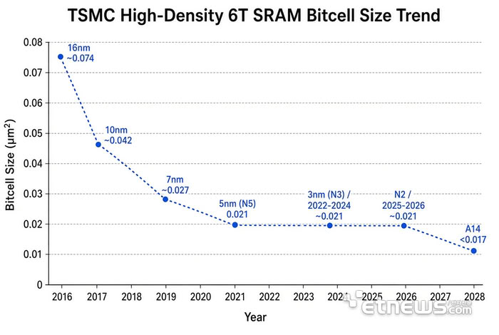
Forward motion on SRAM miniaturisation at TSMC has been absent for a long stretch. After the N5 5nm process reached volume production in 2020, the 6T cell area held at roughly 0.021 square micrometers and has stayed there ever since, while transistor counts per unit area on the logic side kept climbing. Memory simply did not keep up.
What the A14 node changes on the memory side
A14, the node scheduled to reach production in 2028, is where TSMC expects that stall to end. Its 6T SRAM cell is projected at 0.017 square micrometers, a reduction of about 19% from the figure that has held since 2020 — evidence that the underlying technology has been cleared for large-scale manufacturing rather than remaining a paper exercise.
The schedule has been running optimistically, with early progress pulling dates forward. The stage-by-stage picture looks like this:
- Trial production is under way now, used to assess the feasibility of the node and to let customers verify how their designs behave inside TSMC's production environment.
- Risk production is planned for 2027, assuming the trials continue smoothly and no serious yield or manufacturing problems surface.
- Volume production follows in 2028, and A14 is set to be introduced first at the company's headquarters fab in Taiwan.
- Should next year present no obvious obstacles, TSMC may advance the volume start by a few months.
Reading the A14 process against N2
Measured against the N2 2nm node, whose volume production was announced only recently, the step taken by the A14 process is expressed in four headline numbers:
| Dimension | Claimed gain of A14 over N2 |
|---|---|
| Speed at the same power | up to 15% speed improvement |
| Power at the same frequency | up to 30% power reduction |
| Logic | 20% higher logic density |
| Memory | 19% higher SRAM density |
Why both tracks moving together matters
The significance goes past a single decimal point in a cell area. What A14 sketches is a generational step in which logic circuits and memory shrink at a comparable scale, a situation that contrasts sharply with the pre-10nm era. For engineering teams, the practical reading is straightforward: 0.021 can now be filed away as the old baseline, while 0.017 becomes the figure to plan around once the node starts volume output at that Taiwan headquarters site in 2028.