
ItInsightsWorld General Brief: Stanford University Diamond Transistor Work Points To 50x Faster Switching
Switching speed with diamond as semiconductor
An all-diamond transistor effort developed with Stanford University uses diamond as the semiconductor medium, and the switching-speed target attached to the collaboration is 50x faster.
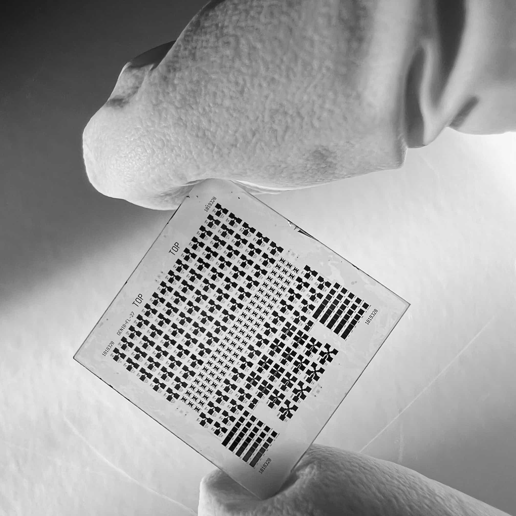
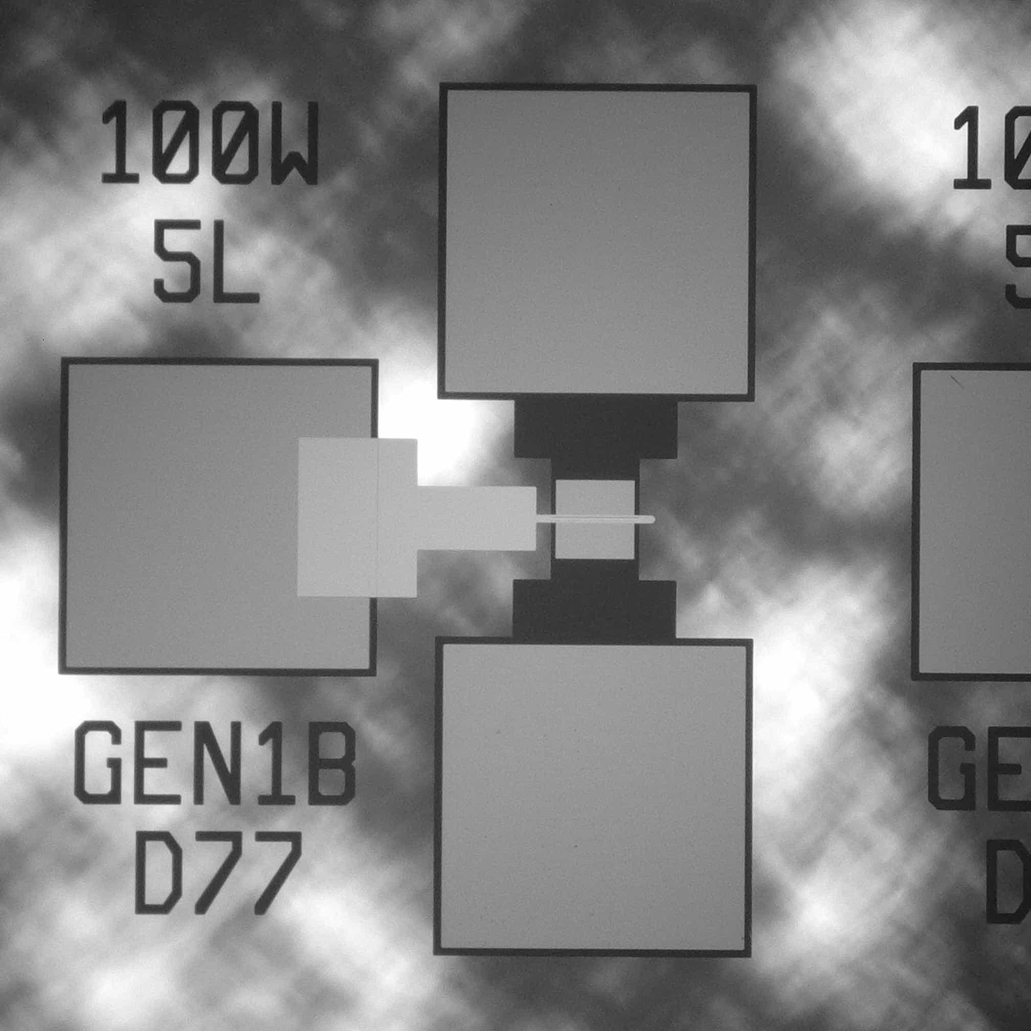
Creating carriers at the surface
The charge carriers are produced without putting substitutional dopant atoms inside the bulk crystal. In these DF devices, surface transfer doping supplies the carriers.
IEEE paper describes the mechanism
A DF Paper in IEEE: On the Conduction Mechanism in Diamond 2-Dimensional Hole Gas Field Effect Transistors explains that hydrogen termination of a single-crystal diamond wafer surface can make electron affinity negative.
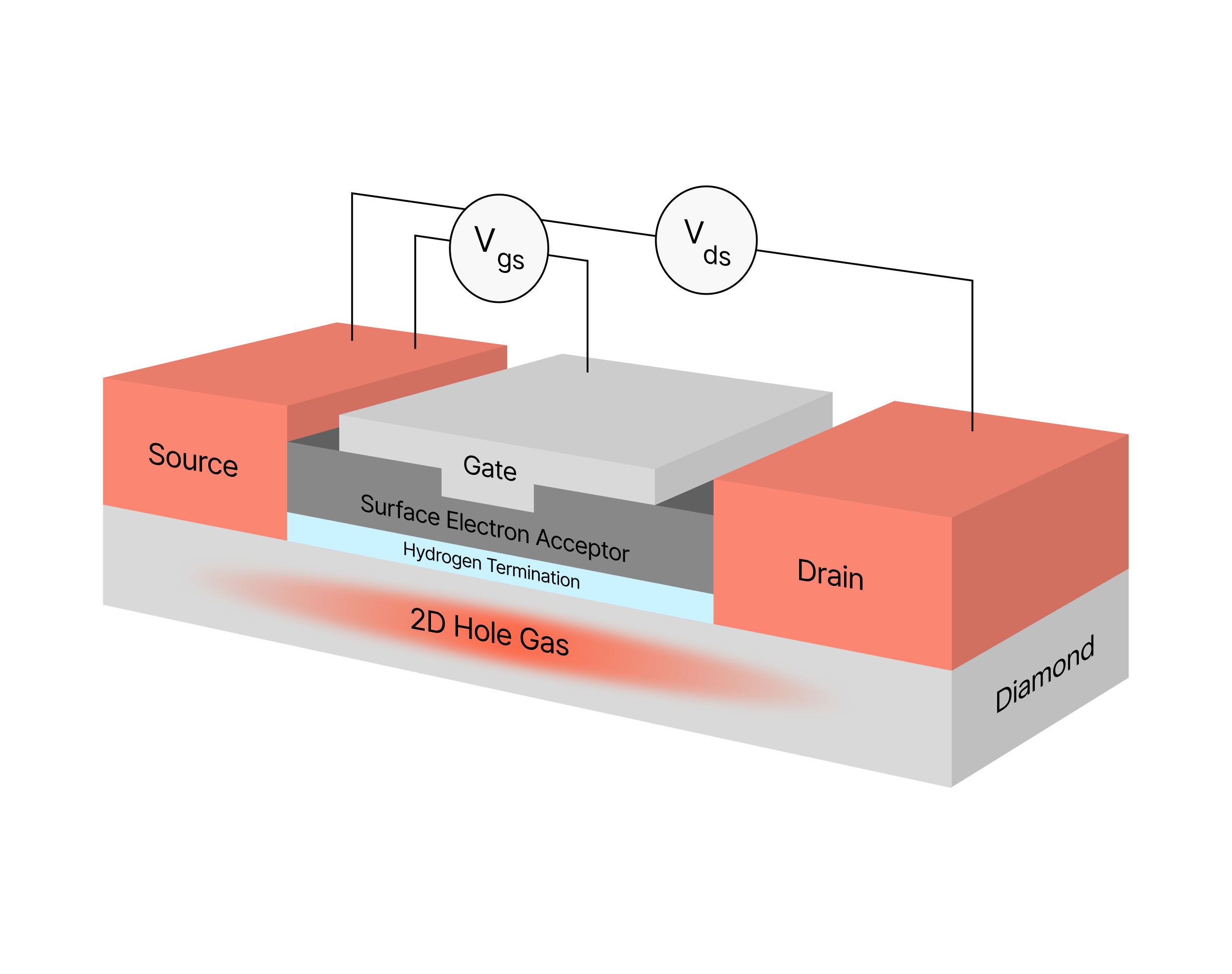
Once that surface state exists, electrons may leave the diamond valence band and move to suitable acceptor species, often adsorbates or engineered surface layers. The transferred charge creates a high-density two-dimensional hole gas, 2DHG, confined within a few nanometers of the surface.
The result is p-type conductivity while the diamond bulk keeps intrinsic purity, thermal conductivity and breakdown strength. Because ion implantation and lattice substitution are not needed, defect generation and carrier scattering associated with conventional doping are avoided, supporting high-power, high-frequency and radiation-hard electronic platforms.
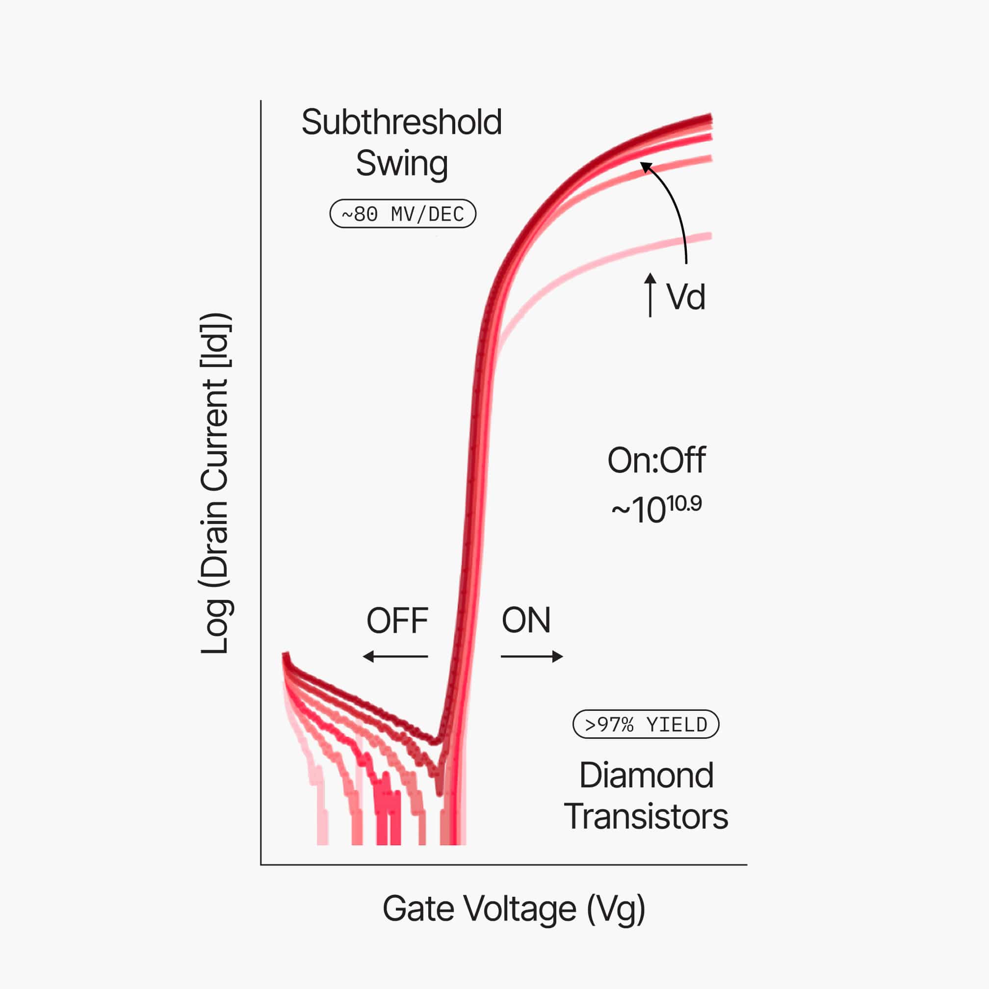
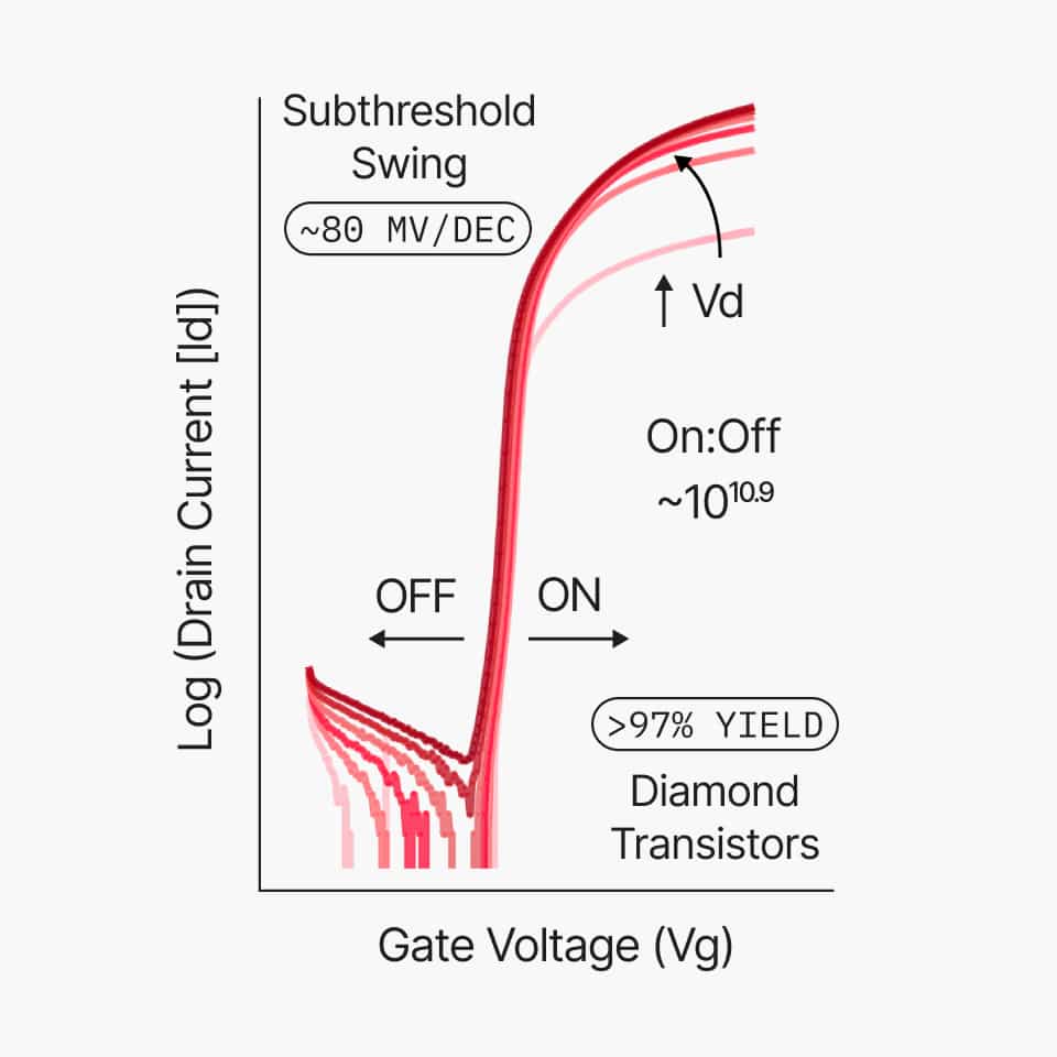
Subthreshold swing reaches 3 nm silicon parity
DF devices now match state-of-the-art 3 nm silicon in subthreshold swing.