
When Simulation Runtime Blocks AI Silicon: NVIDIA cuLitho and Siemens Calibre Target 10x to 17x Speedups
When full-chip patterning verification starts to strain production schedules, the limiting factor is often compute. Siemens and NVIDIA are responding by combining NVIDIA cuLitho, a CUDA-X library, with Calibre manufacturing software. Verified engineering data cites 10x to 17x simulation speedups for key workloads, and the collaboration describes at least 10x to 17x gains for critical lithography simulation tasks.
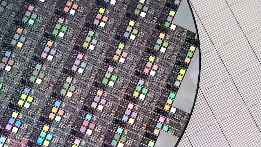
Why advanced patterning meets the runtime wall.
Leading-edge process nodes make lithographic patterning increasingly complex. High-NA EUV manufacturing and curvilinear methods such as Inverse Lithography Technology (ILT) demand far more computation than traditional optical proximity correction (OPC) workflows can handle comfortably. The result is a runtime wall. Without acceleration, full-chip, manufacturing-scale deployment can become too slow, pushing engineering teams to balance optimization depth against project deadlines and increasing the risk of lithographic hotspots or reduced process margins.
How cuLitho and Calibre attack simulation time
The Siemens and NVIDIA effort is aimed at a concrete constraint: lithography simulation runtime. NVIDIA cuLitho, a CUDA-X library built for GPU-accelerated computational lithography, is integrated with Calibre manufacturing software. The collaboration states at least 10x acceleration for key lithography simulation workloads, with verified data supporting at least 10x to 17x speedups. That change is intended to make fuller optimization and earlier hotspot detection feasible before tapeout.
Measured implications for chip and photomask makers
For semiconductor and mask manufacturers, the value is tied to workflows that must complete at production scale. The collaboration reports measurable performance gains across critical computational lithography tasks. Verified engineering data supports at least 10x to 17x simulation speed-ups for key workloads, making full-chip curvilinear patterning more practical for High-NA EUV production.
What saved compute time changes
- Earlier hotspot detection: shorter simulation times allow potential lithographic hotspots to be identified before tapeout.
- Deeper optimization: manufacturers can run more comprehensive optimization cycles within the same schedule.
- AI silicon readiness: faster turnaround can support manufacturing readiness for next-generation AI semiconductors and memory devices.
The significance is not limited to a benchmark figure. By connecting a CUDA-X library with Calibre manufacturing software, Siemens and NVIDIA are directly addressing the runtime wall. For the most demanding patterning checks, the result may give semiconductor makers more time, more iterations, and clearer visibility into process margins for High-NA EUV and ILT workloads at manufacturing scale.