
AMD Fills Samsung's Taylor Fab 2: A Q&A Decision Guide to the HBM Base-Die Rush
Lead with the conclusion, because the headline is easy to misread. Samsung Electronics' foundry arm is no longer the division that has to chase American customers for wafer slots. According to National Business Daily's November 3 report, drawing on Korean industry media, the company has won AMD's order for the base dies of its next-generation high bandwidth memory, to be produced at the planned second fab in Taylor, Texas — and that same plant is already close to fully booked, with AMD taking the majority of the planned output. For readers outside semiconductors, this is a cleaner signal than any product launch: the AI hardware bottleneck has shifted from "who builds the fastest chip" to "who controls the nodes, the slots and the packaging capacity four or five years in advance." Here is the story broken into the questions people actually ask.
Three takeaways if you read nothing else
- The order is a bridge, not a trophy: one product connects Samsung's memory franchise with its advanced logic foundry capability.
- The clock is long: main construction is expected to begin in November 2026, equipment installation from February 2029, and commercial mass production in 2030.
- The confirmation level is low: no customer names or capacity splits have been published by the company, so allocation details remain media reporting.
Q1: What is an HBM base die, and why did it become a foundry product?
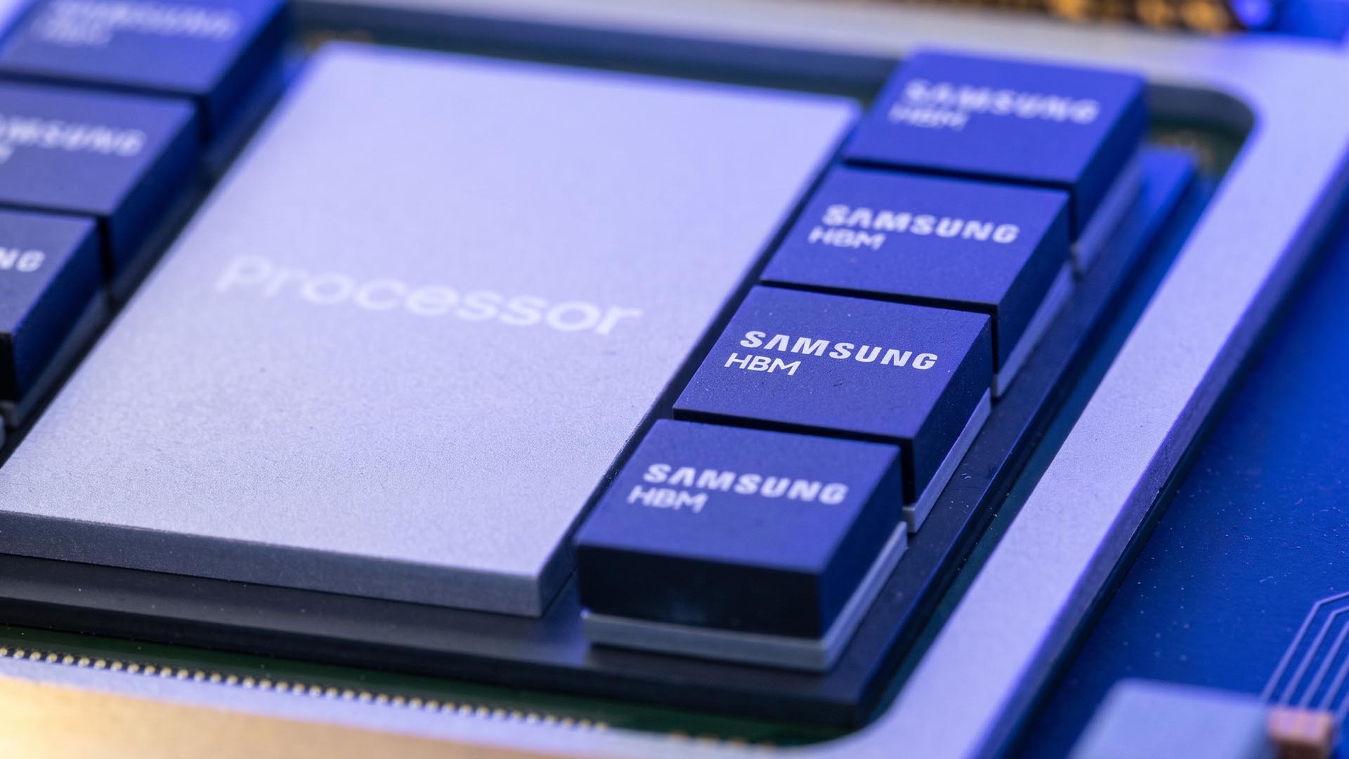
HBM is not simply a stack of DRAM chips glued together. At the bottom of every memory stack sits a base die that manages the traffic inside the stack and handles the control logic that talks to the processor. As the technology generations advance, that little chip matters more and more: its design and its manufacturing process directly shape memory bandwidth, power consumption and overall performance.
This shift is now written into the spec sheet rather than left to each vendor. JEDEC published the HBM4 standard, JESD270-4, in April 2025, moving the interface to 2,048 bits and pushing base-die design onto logic processes so it can carry far more control circuitry. That single change explains the news: memory makers can no longer do everything inside a DRAM fab, so they have started behaving like foundry customers.
Q2: Why does this particular AMD order matter so much for Samsung?
Over the past few years, Samsung has fought TSMC hard in advanced logic nodes and has consistently struggled to win equivalent customer recognition in high performance computing and AI accelerators. An HBM base-die order from AMD gives Samsung something a marketing campaign cannot buy: a reason for a top-tier chip designer to qualify its advanced logic process on a part that sits inside a product where Samsung is already a memory leader. If it works, the company extends its reach inside the AI hardware supply chain without having to beat anyone on GPU design.
Q3: What does the physical production route look like?
The flow is a trans-Pacific assembly line, and the order is really an order for one station on it:
- Base dies are fabricated at Taylor Fab 2 in Texas on advanced logic process.
- Those wafers are shipped back to Korea.
- There, DRAM core dies produced at Samsung's domestic memory plants are stacked and advanced-packaged with the base die.
- The finished HBM units go to the customer, to be integrated with its accelerators.
The logic behind this division of labour is straightforward: it combines American wafer foundry capacity with Korean memory manufacturing depth, instead of forcing one site to do both well.
Q4: How big is Taylor Fab 2, and when will it actually run?
| Dimension | First Taylor plant | Taylor Fab 2 |
|---|---|---|
| Scale | Baseline for comparison | About 2.7 million square feet, roughly 1.5 times the first Taylor plant |
| Status | Equipment installed and 2nm trial production getting under way; reported initial wafer input of about 50,000 wafers per month | Site preparation finished; main construction expected to start in November 2026 |
| Key dates | Trialling 2nm-class production now | Equipment installation from February 2029; commercial mass production in 2030 |
| Reported customers | Tesla automotive chips | AMD (majority of planned capacity, as reported), with Nvidia also named |
| Process | 2nm | 2nm and more advanced manufacturing |
Two points of context from outside the original report. First, Korean trade and tech media said in September 2026 that the first Taylor plant's 2nm capacity was already fully reserved before trial production, with orders including Tesla's AI5 chip, a next-generation Broadcom communications part and an Arm-side AI chip — which is why the second site is being pulled forward. Second, the new fab targets 2nm and more advanced processes precisely because next-generation HBM base dies need logic-class density and energy efficiency; unlike traditional DRAM, a base die is a logic chip, and that is what makes it contested foundry business.
Q5: So is Nvidia on board? Read the catch
AMD is not the only name attached to the plant. Korean media reported that Samsung has received orders covering the entire planned capacity of the facility, with Nvidia among the customers — although AMD reportedly accounts for the bulk of it.
Nvidia's position is more complicated. Earlier reporting indicates that Nvidia would like its memory suppliers — Samsung, SK hynix and Micron — to have the base dies for its next-generation customised HBM produced uniformly through TSMC, so that parts from different vendors share one manufacturing process. The reasoning is practical rather than political: fabs differ in process, power and thermal behaviour, and if each memory maker uses a different base-die supplier, Nvidia must spend extra time on verification and adaptation. A single source reduces performance spread between suppliers and lowers the difficulty of developing customised HBM. Reporting from TrendForce on October 19, 2026 put the same request in more specific terms, describing Nvidia pushing TSMC's 3nm node for NVHBM base dies across the three memory makers.
The consequence for readers: winning AMD does not automatically hand Samsung equal standing in Nvidia's customised HBM chain. Samsung is still qualifying its own advanced wafer foundry process, hoping to prove it can meet the requirements of products such as NVHBM. If Nvidia's demand eventually outgrows what TSMC can supply, the plant in Texas becomes the most credible alternative route — which is exactly why a factory that will not mass-produce until around 2030 is already being discussed as scarce.
Q6: How tight is this capacity really? Three reference points
- Base dies are already consuming leading-edge capacity today, before Fab 2 exists. Reporting in September 2026 said Samsung's 4nm line was running at full load, with roughly 50% to 60% of that output allocated to HBM4 base dies — on the order of 15,000 wafers a month equivalent.
- Memory and logic are now competing for the same wafers on the DRAM side as well. A Samsung executive vice president said on September 29 that HBM would take close to 30% of DRAM makers' total wafer capacity next year, up from about 20% now.
- Forward bookings have become the norm. In its third-quarter 2026 earnings call on October 29, Samsung told investors its 2027 HBM supply was already sold out at agreed target prices, with overall DRAM supply still tight into 2028.
Read together, these explain why "nearly sold out" is not marketing language in this market. Capacity is being allocated years ahead of demand, which is what eventually shows up in product schedules and prices.
Q7: What is confirmed, what is reported, what is unknown?
- Company statement: Samsung said only that it cannot confirm customer-related information; no official contract detail has been published.
- Reported, not confirmed: the AMD HBM base-die order and its share of Fab 2 capacity, plus Nvidia's presence among the customers, all trace to National Business Daily's November 3 report and Korean industry media.
- Still unknown: exact order volume, pricing, which process node AMD's base die will use, and whether Nvidia has committed any purchase rather than merely reserved optionality.
Common misconceptions
- "Booked capacity means guaranteed chips." Reservations precede qualification. A customer can hold slots at a site that has not yet demonstrated yield, and can walk if it does not.
- "This is Samsung beating TSMC." The same news cycle shows Nvidia leaning on TSMC for base dies; the realistic picture is split sourcing, not replacement.
- "HBM is a memory story." The base die is logic, which is why a foundry business is being built around a memory product.
- "American fabs mean Korea loses the work." The disclosed route keeps stacking and advanced packaging in Korea; Texas supplies the logic layer.
FAQ: the questions readers send us
Does this end TSMC's lead in AI logic? No. It creates a second qualified source at 2nm and more advanced manufacturing, in a category — memory base dies — where Samsung already holds domain strength. Competition narrows at the edges first.
Will any of this make my laptop or phone cheaper? Not soon, and in the near term possibly the opposite. HBM competes with conventional DRAM for the same wafer input; when the share heading into HBM climbs from roughly 20% toward nearly 30%, ordinary memory supply tightens.
Should a business buying AI compute act on this? If you are planning accelerator purchases for 2027 and 2028, the relevant fact is that memory supply is already being contracted at agreed prices. Treat availability as a multi-year negotiation rather than a quarterly one.
What is the simplest way to judge whether this story is real? Watch for official confirmation of a named customer and a production start, not for further reports about reservations.
Action list: five checkpoints to watch before 2030
- November 2026: does main construction actually begin at Taylor Fab 2 on schedule?
- 2027 to 2028: do Samsung, AMD or Nvidia convert media reports into disclosed contracts, and does Nvidia's customised HBM qualification ever add a second source?
- February 2029: equipment installation is the first hard signal on the base-die manufacturing plan.
- 2030: commercial mass production, and whether yields let Samsung take base-die volume from TSMC.
- Continuously: the share of DRAM wafer capacity flowing to HBM — the number that leaks into memory prices long before it appears in headlines.
The wider lesson for anyone watching technology markets is about sequence. Accelerators and packaging get the headlines, but the fight described here is over a chip nobody buys by itself, made on an advanced process at a plant that will not produce until around 2030, in a state where the customers are already arguing about who holds the slots. When a supply chain begins reserving capacity that far in advance, prices, product cycles and bargaining power follow the capacity — not the specification sheet. Keep that framework long after this particular order is confirmed or denied.