
Nvidia Reassesses Rubin Memory Strategy: 8-Layer HBM4 May Balance Yield and Cooling
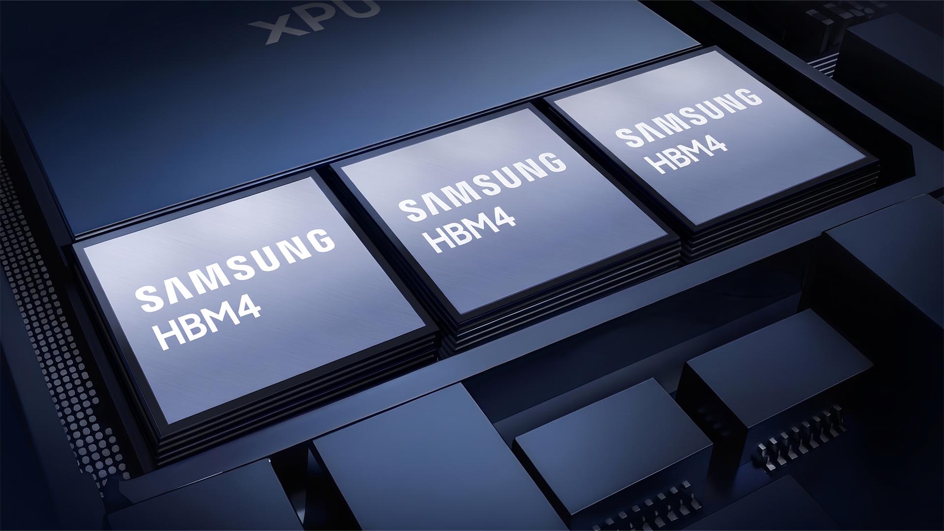
According to recent industry coverage, Nvidia opened discussions with Samsung and SK hynix in Q3 2026 to evaluate a larger role for 8-layer HBM4 in upcoming products. Earlier market assumptions pointed toward the Rubin series relying heavily on more advanced 12-layer HBM4 or HBM4E memory, but supply-chain realities have prompted a review.
Why the manufacturing constraint matters
- Thermal pressure rises with every layer: as a DRAM stack adds one layer, thermal resistance increases, making heat removal harder.
- Yield becomes less forgiving: wafer bonding has a higher chance of defects as stacking complexity increases.
- 8-layer stacking offers a practical compromise: although single-stack capacity is lower than in taller configurations, it is easier to manufacture and cool, supporting cost, capacity and stability goals.
12-layer HBM4 remains part of the roadmap
The review does not imply that Nvidia will abandon 12-layer HBM4. Samsung and SK hynix are currently producing 12-layer HBM4 products that have received Nvidia qualification. Over the next several years, 12-layer HBM4 is still expected to hold an important share of the high-end HBM market. From mid-2027, however, 8-layer versions may gain a substantially larger share.
Certification and configuration choices are still under review
South Korean media reporting indicates that Samsung and SK hynix still need independent qualification for 8-layer HBM4. Both companies are preparing the relevant components, materials and quality validation processes. Because the 8-layer approach is technically less complex than the 12-layer approach, industry participants believe subsequent certification should be easier and unlikely to cause major delays.
Nvidia is not limited to 8-layer HBM4. It is also examining an 8-layer HBM4E option. The final memory configuration will depend on design requirements for Rubin Ultra and its NVL rack-scale systems, along with supply capability and total cost.
Rubin Ultra design adjustments
The Rubin Ultra project has also changed. Earlier expectations pointed toward a more aggressive chiplet-scale architecture, but supply-chain pressure led Nvidia to narrow parts of the plan. Reports say Rubin Ultra shifted to a dual-chip design to reduce manufacturing risk and preserve production schedules.
Rubin and Rubin Ultra are planned for 2027 as the next-generation AI computing platforms intended to succeed the Blackwell series. The partial move from 12-layer to 8-layer HBM4 shows the AI hardware sector is no longer optimizing only for headline specifications and stacking height. It is placing more weight on yield, thermal control and dependable supply.