
ItInsightsWorld General Read: ChangXin Verifies 4F² Sample as the Race to 3D DRAM Tightens
A wafer-level proof point for the next memory cell
ItInsightsWorld reads the completed engineering-sample verification as the moment that moves 4F² from a stated roadmap target to demonstrated wafer behavior: the platform’s core performance indicators are described as having reached design expectations on real wafers. The next gate is client verification; once that is completed, the stage of volume manufacturing can open.
Server DDR5 is the first disclosed showcase
ChangXin had previously said it expects to introduce a new-generation DDR5 RDIMM product that integrates 4F² technology by year-end, targeting one of the most application-difficult domains, servers. That makes the sample result more than an internal milestone: it is the base from which a commercially visible memory product is planned.
Where ChangXin stands among global players
Public progress disclosures put ChangXin at the front of the global 4F² engineering push. Samsung and SK Hynix have both identified 4F² as a key direction for development below the 10nm class, but ChangXin has already completed engineering-sample verification. If the next steps proceed smoothly, ChangXin could become the world’s first company to bring 4F² to deployment.
Why the industry treats 4F² as the scaling bridge
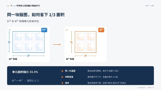
The DRAM road is still driven by density: placing more cells on the same wafer area so the cost per bit can fall. After entering the 10nm class, the older 6F² cell is viewed as difficult to sustain and close to physical limits. The IEEE International Roadmap for Devices and Systems (IRDS) states that when half-pitch shrinking becomes harder, “the transition from 6F² to 4F² cells is the most promising path to maintain cost trends.”
Cell area, platform choices, and the road to 3D
Measured against a minimum lithographic dimension F, the 4F² cell occupies 2F×2F, or about two-thirds of a mainstream 6F² cell. That area advantage has made it a common direction among major memory developers. SK Hynix has positioned its 4F² vertical-gate (VG) platform and 3D DRAM as two key technology pillars; Samsung presented a 10nm-class 4F² paper at ISSCC 2026, and its CTO publicly confirmed R&D work in October this year. The wider industry also regards 4F² as a necessary stage on the path toward 3D DRAM.
Inside ChangXin’s VSG and decoupled architecture
ChangXin’s 4F² scheme centers on its self-developed VSG, or Vertical Surrounding Gate, transistor. Because the gate surrounds the vertical channel, control is stronger, helping reduce short-channel effects and leakage. At the architecture level, the process paths for DRAM and CMOS are separated, then linked through wafer-level hybrid bonding for high-speed interconnect. This allows logic performance, storage density, and reliability to be optimized independently.