
Four GPUs on One Board: What a Giant AMD Prototype Teaches You About Reading Hardware
By James Hartley, IT Insights
Recently a photograph of an enormous AMD graphics PCB began moving through hardware forums and social feeds. The easy reaction is to treat it as a spectacle. The more useful reaction is to ask why anyone would weld four mid-range engines onto a single board, because that answer explains how silicon gets repurposed for a specific workload — and it hands general readers a repeatable template for judging hardware claims.
The conclusion first: the board integrates four Radeon RX 470 graphics cores, carries 32GB of GDDR5 memory and accepts current through four 8-pin power connectors, yet it exposes only one HDMI display output and links to the motherboard over what appears to be a PCIe x8 connection. Each of those details points away from gaming and toward either engineering validation inside AMD or a compute-only duty such as cryptocurrency mining back in the Polaris era.
Five things worth knowing up front
- A genuine AMD board that never reached shelves: the logo on the PCB, the model marking and the Polaris-era silicon all say prototype, not product.
- Four Radeon RX 470 cores arranged in a square, each with its own 8GB of GDDR5 — the 32GB total is four separate pools, not one shared frame buffer.
- On paper the four-GPU design adds up to 8192 stream processors, the same headline figure AMD once shipped on a dual-chip flagship.
- One HDMI port plus an apparent PCIe x8 interface are the strongest clues that games were never the target.
- Why it matters beyond nostalgia: the same "recombine mainstream parts for one job" logic is still active, as old GPU generations keep being pulled back into service.
What was actually photographed
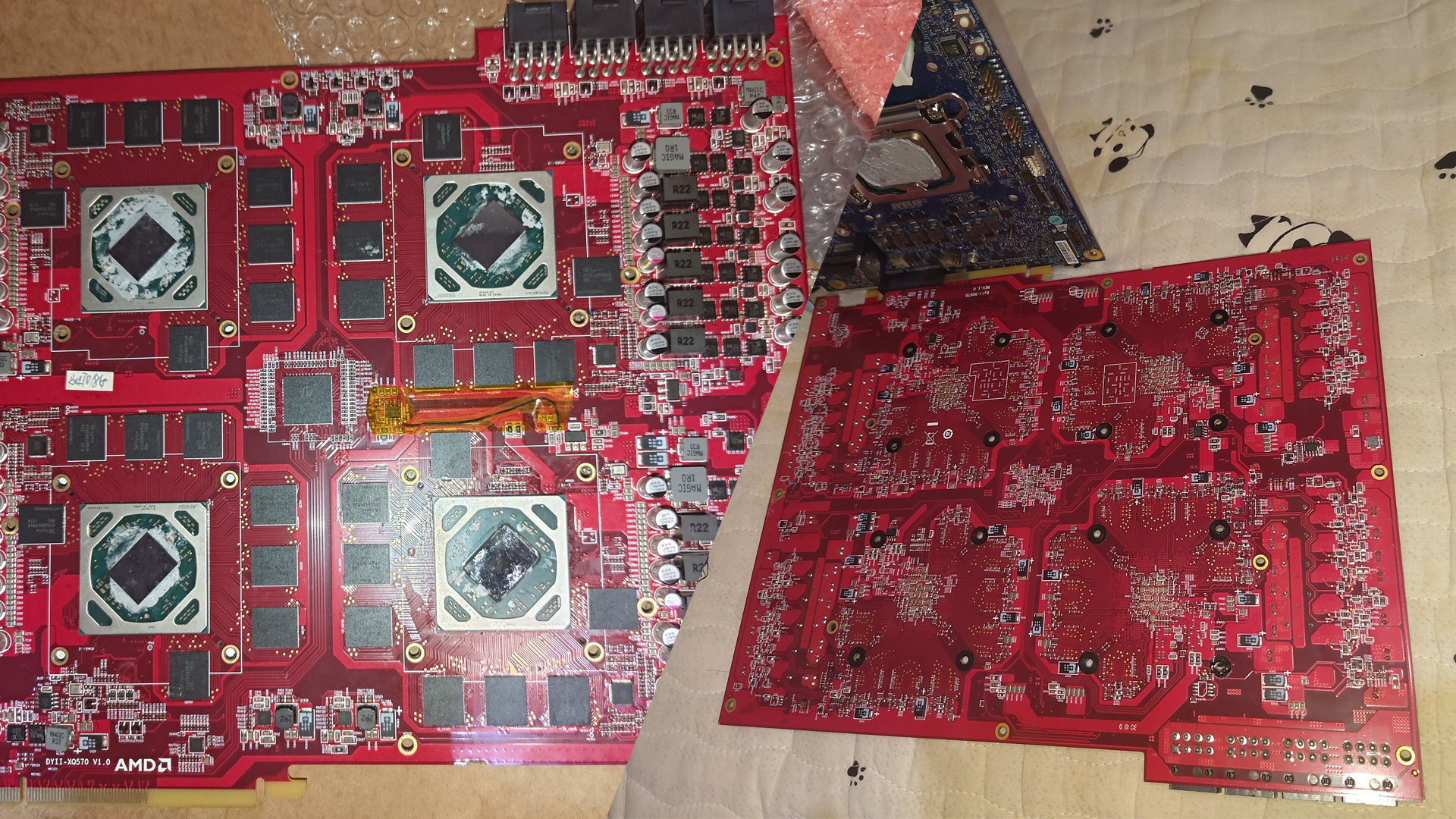
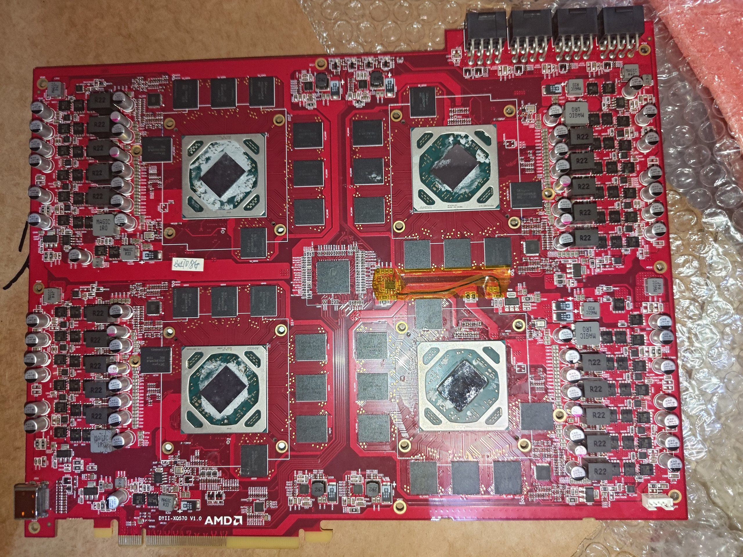
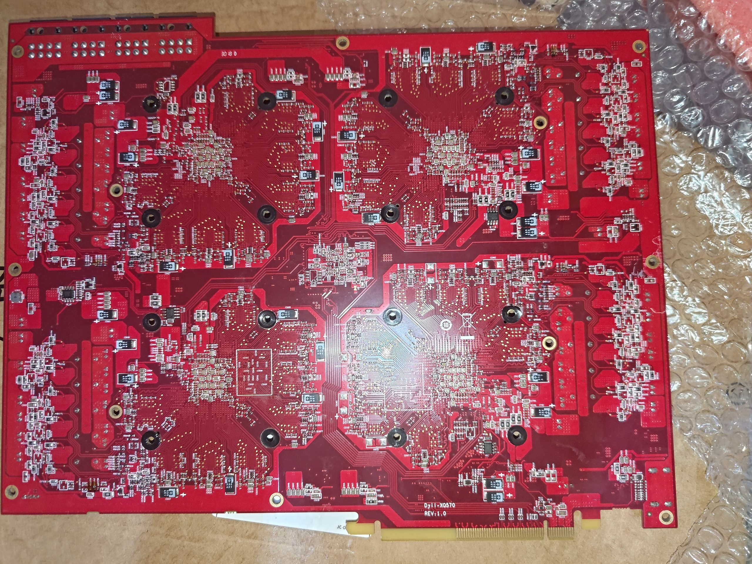
The images were circulated by a hardware leaker known as GOK and picked up by outlets including VideoCardz. The PCB is marked "DYII-XQ570 V1.0", but the person who shared it clarified that the silicon soldered to the board is four Radeon RX 470 GPUs rather than the RX 570 the label implies. Each of the four packages is ringed by eight memory chips; that reporting identifies them as SK hynix GDDR5 devices of 1GB capacity apiece, which works out to a dedicated 8GB per core and 32GB across the whole board, with no memory sharing between the four GPUs.
The layout is where the intent leaks. Four graphics processors demand four independent supply stages, so the board carries power circuitry far denser than any retail card of that generation, fed through four 8-pin auxiliary connectors. Because a single 8-pin connector is specified for up to 150W, the intake ceiling implied by the board works out to roughly 600W before the slot contributes anything. At the same time the video outputs collapse to one HDMI port and the edge connector looks like a PCIe x8 design instead of a full x16.
The arithmetic of one Polaris core
Baseline first. The Radeon RX 470 arrived in 2016, built on a 14-nanometer Polaris 10 design with 2048 stream processors organised into 32 compute units, 4GB of GDDR5 attached over a 256-bit bus, and a typical board power near 120W. Multiplying that by four is what makes the prototype notable rather than merely strange.
| Dimension | One Radeon RX 470 | The four-GPU prototype board |
|---|---|---|
| Graphics silicon | 1 Polaris 10 core | four RX 470 cores on a single PCB |
| Stream processors | 2048 | 8192 in theory |
| Memory | 4GB GDDR5, 256-bit bus | 32GB GDDR5 as four independent 8GB pools |
| Manufacturing node | 14-nanometer | Same generation, four dies on one board |
| Power | about 120W typical | four 8-pin inputs, near 600W theoretical ceiling |
| Display output | HDMI plus DisplayPort on retail cards | one HDMI only |
| Host interface | full PCIe x16 slot on retail cards | appears to be PCIe x8 |
| Market status | mass-market part of its era | never announced, never sold |
Four clues that this was never a gaming card
- Output count. A card built to render frames has to hand those frames to a screen. One HDMI port cannot support the multi-monitor setups that justify an oversized board.
- Bus width. A PCIe x8 link throttles traffic between system memory and the graphics processors, which modern games feel immediately.
- Memory topology. Four isolated 8GB pools suit four identical parallel tasks; a gaming engine wants one large coherent frame buffer instead.
- Power and cooling mismatch. Roughly 600W of intake with no visible consumer-style cooling or output array suggests a machine-room or bench environment, not a desktop gaming rig.
Stacked together, these are the fingerprints of hardware built to chew through numbers rather than draw pictures. Nothing in the photograph suggests AMD ever planned to put this in front of consumers.
AMD's own multi-GPU record makes the board stranger
Multiple processors on one card were not foreign to AMD. Its Radeon Pro Duo flagship paired two Fiji GPUs, and published specifications list 8192 stream processors in total at a 350W rating, with the card reaching retailers in April 2016 at $1,499. Two years earlier the same company had already shown it could bridge chips on one board; two years later, at NAB in April 2017, AMD announced a second-generation Radeon Pro Duo built around a pair of Polaris-class graphics processors and fitted with 32GB of GDDR5, priced at $999 and rated at 250W according to AMD's launch material and the TechPowerUp database entry.
That shipping product is the key to reading the prototype. AMD plainly knew how to put two mid-range Polaris GPUs and a large GDDR5 pool onto one retail board. The experimental design with four Polaris GPUs pushed the same recipe to its logical limit and still never appeared in a catalogue — which is why observers call it one of the largest and most unusual PCIe multi-GPU boards to surface in recent years.
Why mining is the most cited explanation, and why it expired
Back then, a quad-core board made commercial sense in one scenario above all: mining. Four identical engines on a single PCB mean one chassis, one power budget, one point of failure and one thing to install — attractive when the work is the same calculation repeated endlessly, and irrelevant when the work is rendering a game frame. That reasoning is exactly why the reduced PCIe link and the single HDMI output stop looking like compromises and start looking like deliberate savings.
The economics behind that logic disappeared on 15 September 2022, when Ethereum completed The Merge, moved from proof of work to proof of stake and ended GPU mining of the network, cutting its energy use by roughly 99.95%, as recorded in Ethereum's own roadmap documentation and reported by PCMag at the time. Industry analysts such as Hashrate Index described the aftermath as billions of dollars of GPU mining hardware suddenly in need of a new purpose — a supply shock that reshaped the second-hand market for years.
Even so, the underlying design conversation has not gone away. Reporting this week describes renewed mining demand and tight supply of current-generation cards pushing some vendors to redirect distribution toward older Radeon models — a reminder that "obsolete" silicon gets re-evaluated whenever a workload needs cheap, parallel, power-bounded compute.
Common misconceptions
- "Four GPUs must mean four times the gaming performance." Multi-GPU gaming depended on explicit game-by-game support that the industry largely abandoned, and the one HDMI output plus PCIe x8 link contradict a gaming reading outright.
- "32GB of memory means one very fast frame buffer." The pools are per-core and independent, so the board does not behave like a 32GB graphics card.
- "A bigger board must be a better product." Size here reflects four dies and their supply circuitry, not speed.
- "This has to be a leaked retail model." The printed marking does not match the installed silicon, and no AMD product line ever listed a board with four RX 470 cores.
A five-step way to read any hardware leak
- Read the label, then verify the silicon. Engineering boards routinely carry project codes that differ from any shipping name.
- Count the outputs first. Display ports reveal intended use faster than core counts do.
- Check the host bus width and compare it against the retail version of the same chip.
- Add up the power inputs and ask what workload would need that headroom — and what cooling would carry it away.
- Cross-check one independent report and one primary specification database before repeating any number.
What this means if you are shopping, building or just reading the news
- Buying older hardware second-hand: assume heavy-duty history until proven otherwise. Inspect the power connectors for heat discolouration, ask whether thermal paste was replaced, and stress-test before trusting it for daily use.
- Building a multi-card workstation today: bandwidth between the board and the rest of the system is the constraint, not just chip count. Confirm the slot generation and lane width your workload needs before buying.
- Reading about unreleased parts: a photograph proves existence, not performance. Treat any capability claim as unverified until someone publishes measurements.
- Watching collector auctions: engineering samples occasionally surface for sale, but expect no warranty, no official drivers and no support path.
- General judgement: when a device looks oversized for its job, ask which job it was actually designed around. That single question resolves most confusing hardware stories.
Frequently asked questions
Is this a real AMD product?
The board carries AMD markings and Polaris-generation silicon, so it is best described as an AMD-related prototype. There is no evidence it was ever scheduled for retail release.
How much memory does it hold?
32GB of GDDR5 in total, split into four independent pools that do not exchange data between the GPUs.
Could it run games at all?
The underlying Radeon RX 470 cores are graphics processors, so the silicon can render. In practice one HDMI output and a PCIe x8 interface make it a poor gaming device, and that was clearly not the design goal.
Why does a decade-old experiment still matter?
Because it shows how manufacturers recombine mainstream parts when a new workload appears. The same pattern explains why older graphics cards keep returning to the market during supply crunches, and why purpose-built silicon now dominates data centres.
Who found it, and where can the details be checked?
The board images were shared by the leaker GOK and reported by VideoCardz; the earlier dual-GPU comparison points come from AMD's 2017 launch coverage and the TechPowerUp GPU database, while the mining-context figures come from Ethereum's own roadmap documentation and contemporaneous reporting.
The bigger lesson
The prototype never reached a shelf, and it probably never will. Its value is analytical: four graphics chips, four separate memory pools, a stripped-down set of outputs and an unusually small PCIe link form a coherent answer to a single question — what does this machine have to do, and what can it safely not do? Once you start reading hardware that way, most headlines about "the biggest card ever" resolve into something far more interesting: an engineer's trade-off, preserved on a red circuit board.
Have a view on this, or a similar artifact worth explaining? Reach IT Insights at contact@itinsights.com.